http://en.wikipedia.org/wiki/Serial_Peripheral_Interface_Bus
This interface works only in master mode.
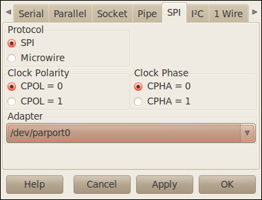
The spi/microwire port doesn't need spi-driver anymore but still uses the same dongle.
Here is the SPI pinout (from the SPI driver doc)
| Pin | Name | Signal | Direction (PC is the master) |
| 1 | Strobe | MOSI | Master -> Slave (Data) |
| 2 | D0 | CE0 | Master -> Slave (Chip Enable) |
| 3 | D1 | CE1 | |
| 4 | D2 | CE2 | |
| 5 | D3 | CE3 | |
| 6 | D4 | CE4 | |
| 7 | D5 | CE5 | |
| 8 | D6 | CE6 | |
| 9 | D7 | CE7 | |
| 11 | Busy | MISO | Slave -> Master (Data) |
| 14 | Autolf | SCK | Master -> Slave (Clock) |
"Here at Paul Elektronik we defined a private standard for the SPI bus on a 10 pin header. You can use it freely. The pinout is given below. It is chosen for two reasons: It minimizes crosstalk and allows for arbitrary many CEs to be used simply by extending the pin header. This extended pin header is still usable by a 10 pin cable, although only the first CE is usable.
Viewed from component side
2 4 6 8 10
_________
|o o o o o|
|x o o o o|
---------
1 3 5 7 9
Pin 1 is cut off and a coding plug is inserted into the female connector on the flat cable. The pins carry these signals:
| Pin | Name | Remarks |
| 1 | - | Cut off to code the pin header |
| 2 | MISO | |
| 3 | GND | |
| 4 | MOSI | |
| 5 | GND | |
| 6 | +5V | If supplied via the cable, NC otherwise |
| 7 | GND | |
| 8 | SCK | |
| 9 | GND | |
| 10 | CE0 | Numbering is relative to the board, not the system |
Each board with SPI chips starts the numbering from CE0. The mapping (connection) between the CEs of the master and the local ones is done via the cabling harness.
If more CEs are used on a board, the pin header is extended as needed with the additional pins being CEs only. Pin 11 is CE1 then, Pin 12 CE2 and so on."